



Sputtering
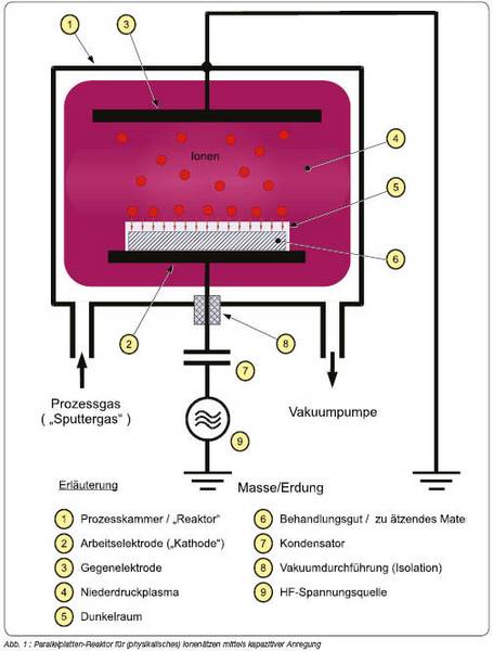
Sputtering is etching by means of ionbombardment. The plasma system for this process is designed as a sputter etcher. In this mode, a working electrode is connected with the plasma generator but capacitively decoupled by means of an intermediate capacitor. Thus, no current can flow between generator and electrode. For sputtering, the reactor is preferably operated at the HF frequency of 13.56 MHz. At this high frequency, the light-weight electrons follow the electric field while the heavy inert ions cannot follow. They remain almost immobile and cold.
Each time positive voltage is applied to the working electrode, electrons collide with the electrode. But because the intermediate capacitor prevents them from flowing off, the working electrode gets an increasingly negative charge. This is the so-called self-bias effect. The substrate is positioned on the working electrode and likewise receives the negative charge. By means of the bias voltage, a DC voltage field is superimposed over the HF alternating field. The DC voltage field then also accelerates the ions onto the now negative working electrode and the substrate. Preferred process gas for sputtering is argon. It does not react chemically so that purely physical etching occurs. The accelerated ions collide with the substrate where they can break atoms, molecules and radicals off the surface, almost independently of the characteristics of the actual substrate. This etching process is referred to as physical etching, ion etching or also micro-sandblasting, because the effect is similar to that of sandblasting, with a grain size reduced to atomic dimensions. Sputtering can clean surfaces from substances of any kind which cannot be removed by other types of plasma cleaning. Furthermore, just like sandblasting it increases the surfaces and improves the adhesiveness.
PVD
Sputtering can also be used to coat substrates by means of physical vapour deposition (PVD).
A target made of the material that is to be coated is placed on the working electrode.
Atoms and molecules broken off the target by sputtering are deposited on the substrate.