

Power modules for efficient power electronicsYour plasma solution for power modules
The benefits of plasma
Power semiconductors are key components in power electronics and the automotive industry. Power semiconductor modules consist of several individual power semiconductors and other components which, together, switch and control high electrical power. IGBTs and SiC MOSFETs act as electronic switches, enabling the rapid switching of currents and thus the conversion of direct current into alternating current. During switching, unavoidable energy losses occur, which must be dissipated as heat. Precise and reliable surface treatment supports crucial manufacturing steps and contributes to stable processes.

Prepared surfaces
Removal of oxide layers or organic residues using plasma
Improved wettability
Plasma activation of the surface energy improves hydrophilic properties.

Better grip
Plasma activation optimises the adhesion of a wide variety of materials
Plasma-assisted manufacturing process
The manufacturing process for modern power semiconductor modules comprises a series of precisely sequenced process steps. Plasma can be used to optimally prepare and optimise the properties of the surfaces. This ensures improved wettability, adhesion, electrical contact and process reliability.

Substrate preparation
A ceramic or metallic substrate serves as the base onto which all individual components are mounted. This usually consists of Direct Bonded Copper (DBC) or Active Metal Brazing (AMB). In order to be able to print the solder paste or silver conductive paste onto it, the substrate must first be cleaned.
| Challenge : Oxides and organic residues can impair the wetting and adhesion of the subsequent materials. | Our solution – plasma cleaning Plasma cleaning ensures an environmentally friendly and, at the same time, component-friendly method of effectively reducing oxide layers and removing organic residues from the substrate surface. |
Benefit
: A cleaned surface promotes uniform wetting and improves the conditions for stable soldering and sintering processes.

THE Bonding
Activated surfaces for reliable adhesion
Power semiconductors such as diodes, IGBTs or SiC chips are mounted onto the substrate. Following cleaning, high-speed automated machines position the semiconductor devices precisely onto the substrates.
| Challenge :Even the tiniest impurities on the surface, combined with its low surface energy, can significantly impair adhesion between the chip and the substrate. | Our solution – plasma activation : Plasma pretreatment cleans and activates the surface prior to the next processing step. |
Benefit
: The increased surface energy creates optimal conditions for a reliable bond and supports reproducible bonding processes.

Soldering or sintering
Ultra-clean surface for electrical and mechanical connections
The electrical and mechanical connection between the components and the substrate is thermally bonded. This bonding is achieved by reflow soldering or silver sintering. In reflow soldering, the components are thermally bonded to the substrate. In silver sintering, a highly durable connection is formed under temperature and pressure.
| Challenge :The electrical and mechanical connection can be compromised by oxides and organic residues. | Our solution – plasma cleaning :Plasma removes oxides and organic compounds and prepares the surface for the subsequent process through cleaning. |
Benefit
: Optimal conditions for wetting and bonding enhance the reproducibility of the process.

Wire-Bonding
Optimised surface for reliable electrical contacts
The contacts on the top of the chips are electrically connected to the conductive tracks on the base substrate. Aluminium or copper wires are used, depending on the application.
| Challenge :Organic contaminants and oxides on the surface can significantly affect bondability. | Our solution – plasma activation: Targeted plasma cleaning and activation of the surface prepares it for ultrasonic bonding. |
Benefit
: Optimised surface conditions support stable bond connections.

Housing assembly and connections
Improved adhesion for reliable housing assembly
The populated substrate is soldered onto a copper base plate. The substrate is mechanically protected by a heat-resistant plastic frame acting as the housing. The main connections are soldered, welded and pressed into place using a press-fit process.
| Challenge :Unreliable adhesion between the substrate and the housing can compromise the reliability of the connection. | Our solution – plasma activation: Plasma activation improves the surface energy prior to further bonding processes |
Benefit
: Increased surface energy guarantees reliable adhesion.

Encapsulation
Preparing
three-dimensional surfaces specifically for encapsulation The module is protected against moisture, dirt and electrical arcing and is encapsulated with silicone gel or overmoulded with epoxy. The housing is filled with silicone, which remains flexible after curing to absorb thermal stresses. In electric cars, the module is alternatively completely encapsulated in epoxy resin.
| Challenge :With complex three-dimensional components, poor adhesion between the housing and the encapsulation material can lead to weak points. | Our solution – plasma activation :A plasma treatment activates the surface prior to encapsulation, thereby optimising adhesion. |
Benefit
: The increase in surface energy achieved through plasma activation ensures reliable adhesion of the encapsulant.
Plasma in the power module manufacturing process
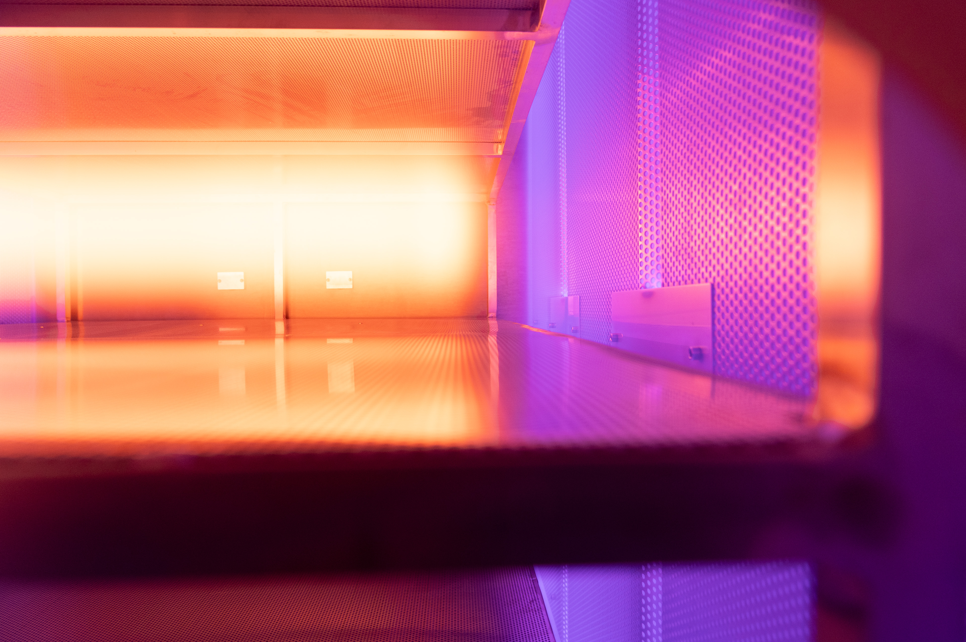
High-performance power modules such as IGBTs or SiC MOSFETs are subject to the stringent performance requirements of various industries, including reliability and quality at each stage of the manufacturing process. Diener electronic supports these processes with precisely tailored plasma treatments. Depending on the process step, plasma is used for cleaning, oxide removal and surface activation. Plasma treatment specifically prepares critical surfaces for subsequent processes such as soldering, gluing or bonding. For surface treatment, Diener electronic offers low-pressure plasma systems capable of using various process gases and gas mixtures, such as hydrogen or argon-hydrogen mixtures. Gas consumption is lower than, for example, in processes using atmospheric-pressure systems that run on nitrogen as the process gas. Plasma technology removes oxide layers that are already present or that form during previous steps of the process. Other organic residues that arise after sintering, such as fluorine, can also be removed using plasma.
A sound investment
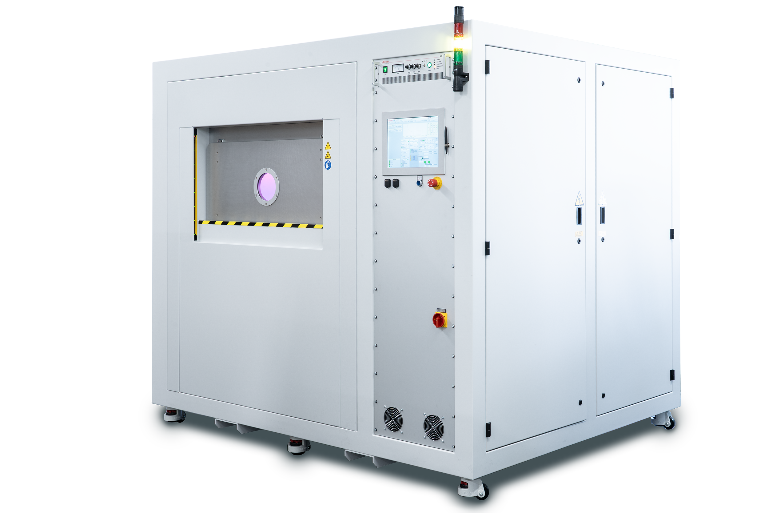
With years of expertise behind it, Diener electronic can draw on a wealth of experience in plant engineering spanning a wide range of industries. Specialising in sophisticated processes, Diener offers a bespoke solution for every application. The design of the plasma systems ranges from partially to fully automated and adapts flexibly to the increasing demands of Industry 4.0. As a secure investment for the future, Diener configures the plasma systems to suit its customers’ production environments. Connection and full integration into an MES via OPC UA are made possible by features such as an automatic door or bell. The plasma systems feature an intuitive user interface that allows for the archiving of programmes and processes, alarm lists and real-time status monitoring, enabling transparent traceability of individual parts. This guarantees reliable, reproducible process flows. For integration into existing production environments, Diener electronic offers high-frequency plasma systems. The solution for the requirements of automated and cycled manufacturing processes.