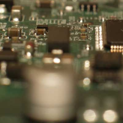
Etching printed circuit boards
To attach the conductors to a printed circuit board, photolithography processes are used. Here, plasma technology comes in at different steps. First, a metal coat is applied over the entire surface, and a photoresist layer on top of it. The photoresist layer is exposed and developed. The structure of the what is to become the conductors remains covered with photoresist. Next, the metal coat is removed from the uncovered areas by reactive ion etching (RIE).<br/>Finally, the photoresist on the conductors is removed by plasma etching in the oxygen plasma.
