
Our company offers many different plasma processes and parylene coatings. Our process development department is always at your side to determine which system technology and processes best meet your requirements.
We develop all processes in-house, from simple cleaning to complex coatings. We start by discussing your wishes and requirements in detail so that we clearly understand the task. Next, we do a series of tests and evaluations of different process parameters at sample parts. For this, our Technical Centre is equipped with 30 test plants of different designs.
In cooperation with you, we adapt not only the process parameters but, if desired, also the system components to your requirements. As we construct the systems in-house ("Made in Germany"), we can carry out the conversion of electrodes, product carriers or special superstructures on our own within a short period of time.
3D laser scanning microscope
We use the 3D laser scanning microscope from Keyence to measure surface roughness. The non-contact roughness measurement system uses two light sources: Laser light and white light. With its great depth of field, this microscope is ideal for precise observations and 3D measurements.


Wetting angle measurement

Microscope

SEM

Coat thickness measurement

Tensile testing machine

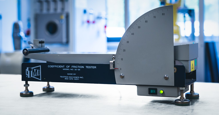
Inclined plane
Test inks
 Set 8 ungiftig farbig Flaschen")
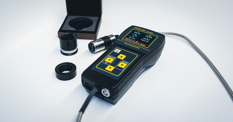
Colorimeter
Plasma indicator

Small parts bulk coating
