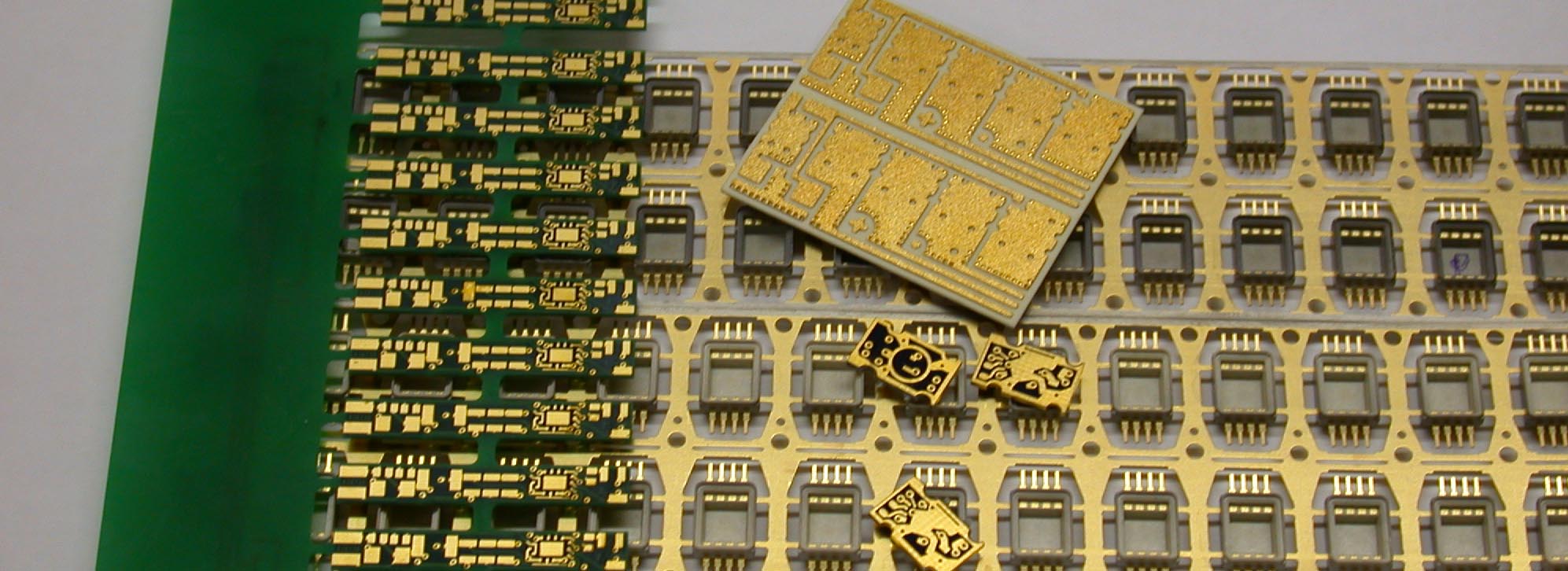
Glossary of surface technology
Printed circuit board etching
Applying the conductors on a printed circuit board is usually carried out by photolithography:
- First, the entire printed circuit board is covered with a conductive layer (metallised).
- Next, a photoresist coat is applied to the entire surface; negative or positive resist can be used. Positive resist is removed where it was exposed during the development process and negative resist remains exactly where it was exposed.
- The photoresist is now exposed with the structure of the desired conductors. If positive resist was used, the areas where the metal coat is to be etched off are exposed; if negative resist was used, the areas are exposed where the conductors are to be.
- After the development process, the photoresist coat remains on the areas where the conductors will be.
- Now the printed circuit board is etched. The photoresist is attacked either not at all or to such an extent that the underlying metal coat remains undamaged. The metal surfaces exposed after removal of the photoresist are etched away, either by wet chemical etching or by plasma etching. The etching rate is higher in the wet-chemical process. However, wet-chemical etching has an isotropic effect so that undercutting of the photoresist mask occurs, i.e. the metal coat of the future conductor will be attacked also from the sides below the photoresist coat. By setting the etching parameters correspondingly, plasma etching can either be isotropic but also anisotropic (see ⇒ Ion etching IE, ⇒ Reactive ion etching RIE), so that the metal coat is actually removed as a sharp image of the photoresist mask.
- After the conductors have been etched, the photoresist coat itself can be removed by plasma etching processes (⇒ Plasma stripping)
